
Moore's Law slowing down opens up opportunities that haven't been there for 50 years: Kirk Bresniker, HPE
San Jose, California headquartered technology giant Hewlett Packard Enterprise announced a $500 million investment outlay for India early this year, which included the manufacture of IoT (internet of things) products in the country. The $30 billion company houses a large portion of its technical workforce in Indian and plans to expand the India headcount by 20% in the next few years.
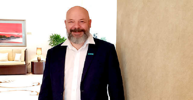
Kirk Bresniker, a three-decade-old HPE veteran, is the chief architect and overall lead for the machine research project at Hewlett Packard Labs, the exploratory and advanced research division of HPE. The project aims to design the first memory-driven computing architecture, an entirely new computing architecture designed to overcome limitations in computing capabilities.
In an interview with TechCircle, Bresniker, who was previously vice president and chief technologist of HP servers' global business unit, spoke about the complicated and specialised world of chip design and architecture and what HPE looks to achieve with the machine research project. He holds 38 patents, including 28 in the US, in the areas of modular platforms and blade systems, integrated circuits, and power and environmental control.
What is your role as chief architect and how instrumental is it as a bridge between the research and business teams?
Being the chief architect at Hewlett Packard labs means I look over all of our development programmes in the labs. The work we do at the labs is applied research as well as the technology transfer within the company into our business units.
Five years ago I was the chief technologist for the server global business unit, which is why I would come frequently to visit the teams here in Bengaluru. We have had a strong engineering presence here for a long time and when I was at the product division, we would look ahead for one or two years. Our roadmaps in the labs team are 10-15 years. And, there's kind of a gap in the middle. That's why after 25 years in the business, I came to this role that is sort of a middle position to try and understand the technology that was being developed in the labs that wasn’t quite ready for technology transfer into a particular business unit.
How did you build your research team?
I was able to pull teams from the business units, hardware teams from our teams, all of our software and operations teams, as well as our field teams from the manufacturing and our services support teams. The idea is how can we take labs' demonstrated work on important problems, that advanced the way people live and work and demonstrate that it is capable or ready to begin the process of technology transfer into the business units. Eight years ago, when I was in my former role as the chief technology officer of the global business unit, my particular area was our mission-critical, our fault-tolerant computing platforms.
And, that was the technology that we have really been working on building up here in Bengaluru, for the better part of 15 years and hence I have long ties into the technology community here.
Over the years, has the time-to-market for an idea in labs to business teams shrunk?
It has become much more complicated. I joined HP in 1989 and back then, I could meet the team that was designing the semiconductor process and architecture that was being soldered to printed circuit boards. And on top of the circuit boards, the operating systems, middleware applications and all that were displayed on an HP terminal, completely vertically integrated.
What that meant was that work that was being done in the labs could find a technology transfer point anywhere up and down the stack.
It was common back then, for someone to work on something in the labs and then follow it into a business unit, whether that was the existing business unit or something that we were starting up. So there was a permeable back and forth between the business units to labs and labs to the business unit. You can innovate anywhere in the semiconductor process, all the way up through to the end-user application. As we grew larger and the supply chain globally became more complicated, it became more challenging.
Because even if you have a great idea to create new microprocessors, we will start talking to Intel, AMD, ARM and so on and it might be three to five years before that technology comes out. You have a great idea and software, well, you would start taking to it the open-source community to see is there someone who's already doing this or talk to one of our long- term software partners like Oracle or Microsoft or VMware. It is like a pendulum, things swing back and forth. In terms of going deeper or specialisation, it doesn't necessarily shrink the timeframe of innovations to hit the market because of the multiple partners involved making it more complex.
Do you see the modern-day innovation focussed more on the software rather than hardware?
Actually, now we are seeing the swing back to more innovation in hardware architecture. And that's particularly interesting for the team that is here in Bengaluru because right now I am getting questions all the time about low-level optimisation of operating systems and hardware architecture. That's what the team here was really great at. And so some of the technologies that they haven't seen for so long like the operating systems, virtualisation technology, all of it is coming back into the foreground.
Also as we transition fundamentally, from delivering products to delivering outcomes and as a service consumption models, that actually opens up and frees us to innovate, much like we used to do earlier.
For instance, if now you are just consuming a service, then I can decide exactly how to execute that service and the ability to be able to deliver that giving the consumers the extra choice. It is a bit of a renaissance in the Silicon Valley for things like silicon hardware design, low-level operating system, firmware and the interface that brings all this together.
Is there any particular reason why the India team was focused on these technologies?
Part of it was understanding how we were maintaining those mission-critical environments. The team here had an affinity for that work. It was a great location to try and maintain and then continue to provide great product service for some of those more mature pieces of software that were the operating system, and even some of the work we inherited when we purchased Compaq. We had all of the virtual memory system (VMS) operating environments. So maintaining the software, and that low-level software capability, was really one of the tasks assigned to the team here in Bengaluru. Now this renaissance in hardware is opening up those skills and technologies and they have been honed here.
When do you decide something requires collaboration with other large companies?
We can do basic research in the labs. A physical fundamental component like our memristor technology and we can decide okay, should this go into accelerators should this go into memory devices or should it go into both. Sometimes the option is we should continue to develop this internally. Sometimes the opposite is like this is a great technology, but we know it has to be bigger than us.
So what is a company or a like-minded group of individuals outside of HPE that we can work together? One example, we have been working for several years on memory semantic fabrics. We co-founded along with a lot of our competitors like Huawei, Lenovo and IBM. It is about finding those common motivating elements that each of us can contribute our knowledge into the consortium and then make it freely available at the license level.
One of the fundamental things we see as an enabler is to have as many people as possible participate in the innovation to have open standards.
You say Moore's Law is getting flattened. What kind of opportunities and challenges does that present?
What Gordon Moore originally said was that about every two years the number of devices you could place in a given area of silicon would double. He said that in 1970 and it was true till about the year 2000. We could essentially photographically shrink. This was called geometric scaling, which ended in the year 2000. The global community realised this in about 1990. They were drawing the graph and they were looking at the devices shrinking and they suddenly realised that if we kept shrinking, by the year 2000, we would have less than one atom.
In some of the devices, you can't have half a silicon atom inside of a transistor. So they realised that we have to do something different. We can no longer shrink the way that we have been shrinking the geometric scaling process. So the global community came together to form an international technology roadmap for semiconductors. And they had about 20 years worth of research and they only had 10 years to do it.
They created the second age of Moore's Law scaling, where the transistors didn't get smaller anymore. But the space between the transistors got smaller. We packed more in the same space. So there were more transistors per unit area. But it wasn't because of what Gordon imagined. Similarly, things began to pop just a little bit above the surface of the chip. So even though the transistors didn't get smaller anymore, because we ran out of atoms to shrink geometrically, we got more devices because the space between the devices struck. So we are at seven nanometres now. That is expected to run out in about five years.
Moore's Law slowing and tailing off actually opens up opportunities that really haven't been there for 50 years. He drew an exponential curve instead of a straight curve. There have been fewer companies who wish to have our own microprocessor architecture and now there are essentially two. And, that is challenging because that means there are fewer design starts, there are fewer opportunities for individuals to contribute at that low level. The semiconductor process is about the same everywhere whether you are going to TMC or Global Foundries or Intel or Samsung.
So, what do we do next?
What we need to do next is to take that transistor on that integrated circuit, and instead of having a life flat on the transmitter on the circuit, as it's done since the very first integrated circuit, we need to turn it vertically, and then do three-dimensional scaling.
Now, this is already available in memory devices. We have 96 layer flash or 96 layers of connections on a vertical device. Unfortunately for us, in our desire to have slimmer cell phones, slimmer peak laptops and greater computation capability, memory components have very low energy density. If I have a gigabit of data inside of a single flash device, accessing every one bit at a time, there is never a dense amount of energy in there. It is distributed across all the possible bits. I can add in redundancy inexpensively. I can do error correction on the data very cheaply in terms of energy and time. If I lose one bit out of a gigabit a flash, I just have lots of spare.
So it is not a question of when we get to three-dimensional scaling, it is, if we do, it is likely to look very different than the kind of microprocessor we are used to. But it is no more about the transistor. That's the only thing we cared about in the past. Faster transistors mean that today's software runs faster too.
Will this space compression strengthen Edge computing over the cloud?
Our expectation is that in the middle of the next decade, 75% of enterprise data will be out somewhere in tiny little embedded devices, in edge systems in successive systems, on the factory floor, in the hospital basement at the bottom of the 5G base station. That's where all the data will be. We have to understand how do we bring the computation out to that data. There's going to be so much more that we will never be able to it bring back to the cloud or to the core on-premise systems.
Even if we have the energy and bandwidth, we wouldn't have the time, because we are talking about things like autonomous vehicles and self-driving drones where you have microseconds in order to analyse data and then take action. Also, it would consume a thousand watts for the autonomous function, and if you are driving an electric vehicle, that's like losing a third of the range.
We have to think of new ways to continue to get more computational work done for much less energy. And also have it fit in the space, weight and power. If I want to have a great machine learning inference engine inside of a flight, a tiny package delivery drone, it can't be based on the conventional technology right now as there is too much heat. It's too much weight and if it takes up too much space, there's no space left over for payload.
What can I do to have a breakthrough? When it comes to aircraft, every gram that I have in the vehicle, that's not cargo, is taking energy, every cubic centimetre that I occupy is space I can't put cargo or people or things and that takes out a bit of battery and my range is less. That means that that vehicle is offline for the charging period. So, how do I have that breakthrough? This is an interesting problem we want to solve.
Next Article