
Lam Research announces chipmaking simulation platform, to train 60k engineers in 10 years
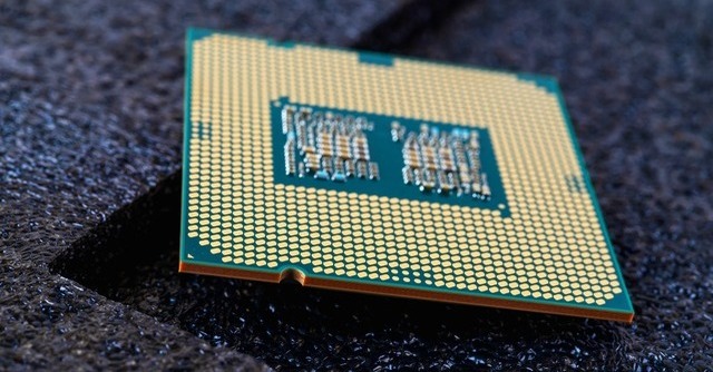
Semiconductor manufacturing equipment supplier, Lam Research, is planning to train 60,000 engineers in India within the next 10 years. The training will be facilitated by the company's virtual nanofabrication environment platform, Semiverse Solutions.
"Lam Research's Semiverse Solutions with SEMulator3D will deliver a virtual nanofabrication environment to help train the next generation of semiconductor engineers in India. Combined with program management and course curriculum customisation, this program is targeted to educate up to 60,000 Indian engineers in nanotechnologies, over ten years, in support of India's semiconductor education and workforce development goals," the company said.
During Prime Minister Narendra Modi's state visit to the US, both the US and India unveiled agreements in the semiconductor industry. One of the notable announcements includes Lam Research’s plan to provide a virtual nanofabrication environment to support the training of future semiconductor engineers in India. The goal is to boost India's semiconductor education and workforce development.
This virtual environment, powered by Lam's Semiverse Solutions with SEMulator3D, will offer a software platform for students to simulate and learn about semiconductor manufacturing processes. By eliminating the need for physical access to a fabrication facility, this approach makes it more affordable and accessible for students to acquire the necessary skills for the semiconductor industry.
During his visit, PM Modi also met several American CEOs, inviting them to increase their investments in India. The executive meeting involved industry leaders like Sanjay Mehrotra, President and CEO of Micron Technology, and Gary E. Dickerson, President, and CEO of Applied Materials.
Micron Technology CEO Sanjay Mehrotra after meeting Modi, as per PTI, said, "We look forward to greater opportunities in India.”
On June 20, the Indian Cabinet approved Micron Technology's $2.7 billion investment plan to establish a semiconductor testing and packaging unit in Gujarat. To support the project, the government will provide production-linked incentives worth $1.34 billion (₹110 billion). This investment is expected to generate 5,000 job opportunities in the country.
Furthermore, following PM Modi's meeting with Gary E. Dickerson, President and CEO of Applied Materials, a US-based semiconductor equipment, services, and software supplier, the company has announced its intention to construct a collaborative engineering centre in Bengaluru. This project will span over four years with a $400 million investment.
The centre is expected to support over $2 billion of planned investments and create 500 new engineering jobs, with the potential for an additional 2,500 jobs in the manufacturing ecosystem, within its first five years of operation. It will primarily focus on developing and commercialising technologies for semiconductor manufacturing equipment.
India is actively promoting the growth of its semiconductor industry and has implemented a production-linked incentive (PLI) scheme to support this initiative. As a result, global companies are expressing interest in investing in India's semiconductor sector.
India is emerging as a prominent hub for electronics and semiconductor manufacturing in Asia. The Indian semiconductor market, valued at $22.7 billion in 2019, is projected to reach $64 billion by 2026, according to a joint report by Counterpoint Research and the India Electronics & Semiconductor Association (IESA).
Next Article