

HCLTech puts ₹185 cr into semiconductor lab as chip ecosystem deepens
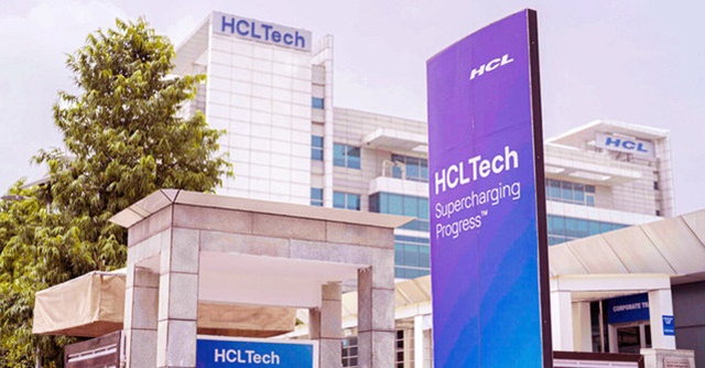
Noida-headquartered IT company HCLTech has invested ₹185 crore in an advanced semiconductor laboratory in Bengaluru, as Indian technology and engineering-services companies expand their presence across the chip value chain amid a government push to build a domestic semiconductor ecosystem.
The 40,000 sq ft facility, which includes 25,000 sq ft of Class 10K and Class 1K cleanrooms, will provide post-silicon engineering, advanced testing, electrical validation, qualification and failure analysis. The third-largest Indian IT firm said the facility is designed to take semiconductor products from specifications to qualified parts, helping customers reduce testing cycles and accelerate time-to-market.
The lab is equipped with automated test equipment and other specialised tools from Teradyne, Advantest, Keysight, Tektronix and Thermo Fisher Scientific. It will serve both domestic and international customers and is expected to pursue certifications including ISO 17025, ISO 9001, AS 9100 and ISO 13485.
“The inauguration of our Advanced Semiconductor Lab in Bengaluru is a proud milestone for HCLTech and reinforces India’s growing leadership in semiconductor innovation,” Hari Sadarahalli, corporate vice-president and global head, Engineering and R&D Services, HCLTech, said. He added that the facility reflects the company's commitment to investing in high-end engineering capabilities and India's ambition to become a global technology hub.
HCLTech's investment comes as peers also deepen their semiconductor capabilities. Infosys acquired semiconductor design company InSemi for a total consideration of ₹198 crore, while TCS has expanded into chiplet-based system engineering and Wipro has partnered with Intel Foundry on advanced-node chip design. L&T Technology Services has also been building semiconductor engineering capabilities as part of its product-engineering business.
The moves reflect a shift in India's IT-services industry from traditional software and embedded engineering services towards specialised chip design, validation and testing capabilities.
HCLTech is simultaneously making a larger infrastructure bet around artificial intelligence. In July, the company announced an initial ₹3,500-crore investment to enter the full-stack AI data-centre business, with plans for an initial 50MW facility through a new subsidiary. The investment will be a mix of debt and equity.
Together, the semiconductor and AI infrastructure investments point to HCLTech's broader push beyond conventional IT services into the physical infrastructure and engineering capabilities underpinning the next wave of technology spending.
India's semiconductor opportunity is also expanding beyond fabs. The government's Semicon 2.0 programme, with an outlay of ₹1.27 lakh crore, seeks to strengthen domestic semiconductor design, manufacturing, packaging, materials, equipment and R&D capabilities.
For HCLTech, the Bengaluru lab provides an opportunity to capture a larger part of that emerging value chain. While chip design has been an established engineering-services opportunity for Indian technology companies, capabilities such as post-silicon validation, testing and failure analysis take them closer to the manufacturing process, and to a higher-value segment of semiconductor engineering.
Next Article