
IBM, Samsung’s VTFET semiconductor design can offer week-long smartphone battery life
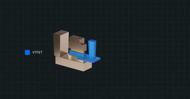
IBM and Samsung have collaboratively announced a new semiconductor design that claims to potentially offer up to 2x performance over present chips, and an 85% reduction in energy consumption. Called Vertical Transport Field Effect Transistors (VTFET), the new semiconductor design entails vertical stacking of transistors on a semiconductor, instead of horizontally.
At present, most advanced chipsets use Fin Field Effect Transistors (FinFET) semiconductor design, which stacks transistors side by side. With VTFET, the current on a chip would move up and down as well as laterally -- thereby improving the overall performance that could be achieved in presently available FinFET processors.
VTFET is one of the ways through which chipmakers are looking to improve the performance of processors, while reducing the size of the semiconductor in use. Intel, on this note, has already spoken about RibbonFET, a technology that it aims to bring into mass production from 2024. VTFET, too, is some time away into the future, and will likely premiere in consumer grade chips from around the same time.
Also read: Google, IBM professional courses most popular in India: Coursera
IBM and Samsung have made a number of tall claims about how VTFET can improve consumer chips. According to the companies, vertically stacking the transistors on a semiconductor base can directly lead to double the performance from a processor based on the present semiconductor size, as it would allow chipmakers to stack significantly more transistors on a chip.
The overall design can also apparently reduce energy consumption drastically, which the two companies state can potentially lead to smartphones lasting for over one full week -- in a single charge cycle. The companies also state that chips based on VTFET technology can enable use cases such as low-power cryptomining, powerful IoT deployments and better data encryption standards as well.
IBM Research states that reduced energy flow through the vertically stacked transistors can help in exponential energy efficiency in chips, without hindering performance. It also states that the new design can help carry on Moore’s Law’s premise, which states that the performance of chipsets can double every year, even as semiconductor sizes are halved.
Next Article